Process Technologies
①Manufacturing technology for high-precision, low-cost ceramic components Achieving
"High Precision × Low Cost" through mass-production know-how
-
<Processing Example 1> Stable quality "mass-production molding technology" – Manufacturing of spark plug insulators –
We mass-produce insulators with stable quality on a manufacturing line where alumina powder is press-molded, ground to the desired shape, and then fired in a continuous furnace. -
<Processing Example 2> Polishing-free "ultra-thin sheet molding technology" – Manufacturing of heat dissipation substrates –
Through our proprietary sheet molding and normal-pressure firing technologies, we manufacture silicon nitride thin sheets with an industry-leading thickness of 0.25 mm without the need for post-processing (polishing).
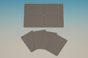
②Manufacturing technology for large ceramic products exceeding 400 mm square
A lineup of "Size" × "Material" tailored to applications
<Processing Example> Vacuum chucks and electrostatic chucks for semiconductor manufacturing equipment components
・Supporting large and special shapes exceeding 12 inches
The Niterra Group has commercialized φ12-inch (approx. 300 mm) sizes, but our unique manufacturing process also enables the production of large items exceeding 400 mm square. In addition to circular shapes, we flexibly accommodate square shapes that increase the degree of freedom in equipment design.
・An extensive lineup of materials to choose from according to the application
Even for large products, you can choose from a variety of fine ceramics, including alumina and zirconia, as well as highly rigid silicon carbide, high-strength silicon nitride, and highly heat-dissipating aluminum nitride.
③Ultra-high-definition, high-precision circuit formation technology on 175 mm large substrates
"Large Area" × "Ultra-Fine" - High-definition circuit pattern formation on large ceramic substrates
<Processing Example> Wiring pattern formation in semiconductor packages
The Niterra Group has established a technology to form extremely fine circuits with a line width and spacing of 20 μm each (L/S=20/20 μm) with high positional accuracy on large ceramic substrates up to 175 mm, flexibly supporting further high-density integration and complex circuit designs for semiconductor packages.

④Complex structure design technology that adds various functions to ceramics
"Molding/Lamination Process" × "Advanced Function Implementation"
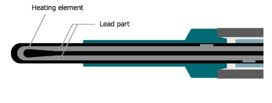
<Processing Example 1> Achieving "ultra-high-speed heating" through the fusion of different molding methods – Manufacturing of glow plug heating elements –
A press-molded silicon nitride insulation part and an injection-molded silicon nitride composite heating element/lead part are integrally sintered using a hot press, finishing in a slender shape of just Φ3.1 mm. This precise structural design achieves a heating function with a temperature rise rate of 1000°C/sec.
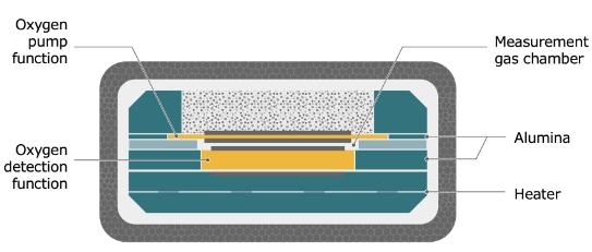
<Processing Example 2> "Extreme condensation of functions" using sheet lamination technology – Manufacturing of oxygen sensors –
Utilizing the Niterra Group's strength in "sheet lamination technology," we form the functions necessary for a sensor—such as a measurement gas chamber, oxygen detection and supply functions, a heater, and electrodes—into a ceramic component measuring approximately 4 mm square.
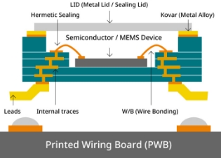
<Processing Example 3> Flexible three-dimensional structure design using sheet lamination technology – Manufacturing of semiconductor packages –
Through our proprietary "sheet lamination technology," we can freely design complex three-dimensional structures such as cavities (structures with a bottom), hole structures, and combinations of these.
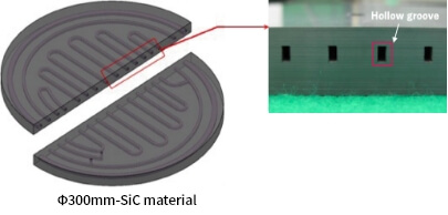
<Processing Example 4> Internal channel formation using adhesive-free joining technology – Manufacturing of semiconductor manufacturing equipment components –
This is a technology to join ceramics together without using adhesives. It is utilized for forming internal channels in components such as semiconductor manufacturing equipment, where the inclusion of impurities is undesirable.
⑤Dissimilar material joining technology
High-durability thermal cycles achieved through "Active Metal Brazing" × "Stress Relief Design"
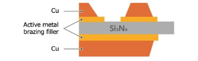
<Processing Example> Robust copper circuit formation using active metal brazing technology – Manufacturing of high heat-dissipating, high-durability wiring boards –
Silicon nitride, which is difficult for metals to wet (adhere to), and copper, which has a large difference in its thermal expansion coefficient. These materials with conflicting properties are strongly joined without voids (pores) using our proprietary "active metal brazing." The greatest feature is that, in addition to a high joint strength of ≧9.8 kN/m, a precise "stress relief design" is applied. By optimally controlling the inclined shape of the side surfaces of the copper plate and the protruding part of the joining brazing filler, we effectively control the stress at the interface. As a result, even in environments subjected to repeated severe thermal cycles, it suppresses the occurrence of cracks and achieves high reliability.
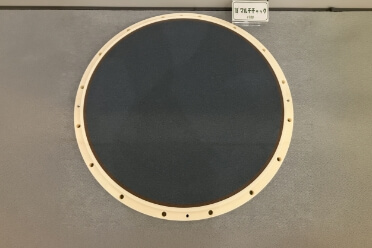
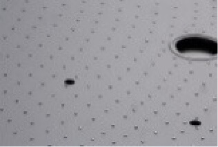
⑥Sub-micron order ultra-flat processing and unevenness formation technology for ceramic surfaces
Surface processing technology that creates "Flatness Precision" × "Flexible Surface Profiles"
<Processing Example> Sub-micron order ultra-flat processing and micro-unevenness formation – Manufacturing of semiconductor manufacturing equipment components –
Using world-class processing technology essential for pin chucks in semiconductor manufacturing equipment, we achieve a flatness of 0.2 μm despite the large diameter of φ12 inches (approx. 300 mm). We can also flexibly accommodate fine adjustments to surface unevenness according to the wafer shape, as well as customization of adsorption zones and pin patterns to enhance adsorption responsiveness. We support major materials such as alumina, aluminum nitride, silicon carbide, and silicon nitride, backing the advanced demands of next-generation processes through the power of materials.
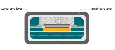
⑦Coating of various functional films onto metals and ceramics
Environmental resistance achieved through "Porous Structure Design" × "Coating Technology"
<Processing Example> Imparting functions through multi-layer film coating – Improving the water resistance of oxygen sensors –
By using a two-layer structure with different pore sizes, we controlled the "capillary force" to form a structure that slows down the penetration rate of water from the outside.