



R&D Interview01
The challenge of electrostatic chucks: Supporting the evolution of semiconductors
from the ground up.

NTK CERATEC pioneers next-generation processes through its unique lamination technology and co-creation with customers.
Semiconductors power smartphones and AI. In their manufacturing, an "electrostatic chuck" is used to fix silicon wafers using electrostatic force, precisely control the temperature, and act as a high-frequency electrode. From the outside, it looks like a single disc. However, inside, it embodies the ceramic technology that NTK CERATEC has cultivated and the challenges of engineers striving to exceed customer expectations. We spoke with Mr. Kameyama and Mr. Tominaga of the Second Technology Development Department about the product's strengths, the story behind its development, and their future goals.
Profile
NTK CERATEC CO., LTD.
Engineering & Development Dept.II Engineering & Development Div. Deputy General ManagerRyosuke Kameyama
Since joining the company, I have been involved in a wide range of activities at the forefront of the electrostatic chuck business, from product and process design to customer support and outsourcing management.
NTK CERATEC CO., LTD.
Production Design Sec.II Engineering & Development Dept.II Engineering & Development Div. Chief EngineerDaisuke Tominaga
I have experience in developing components for semiconductor manufacturing equipment and working as an on-site engineer at client locations. Currently, I am working as a chief engineer on the development of electrostatic chucks.
*The information provided is current as of August 2026.
Organizational structure, names, etc., may differ from the current situation.
The "heart of the device" that determines the quality of semiconductors.
First, what role do electrostatic chucks play in semiconductor manufacturing?
- Tominaga
-
Semiconductors are manufactured by forming tiny circuits on silicon wafers, from which numerous chips are created. One of these processes is etching, which uses plasma/gas to form tiny holes and grooves. Etching is highly sensitive to temperature, and even slight temperature differences across the wafer surface can affect the finished product. Electrostatic chucks hold and secure the wafer using electrostatic force, while simultaneously maintaining a uniform temperature through internal cooling mechanisms and heaters.
- Kameyama
-
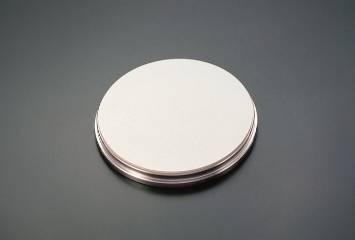
The electrostatic chuck is a component that wafers directly contact within the manufacturing equipment. In other words, its quality directly impacts the quality of the semiconductor chip. Although it looks like a disc, it requires highly advanced technology for ceramic firing and processing, precision machining of metal substrates, and bonding. We consider this to be one of the "hearts" that determine the performance of the equipment.
Because you build upon each other, you can draw freely.
What are the strengths of NTK CERATEC's electrostatic chucks?
- Kameyama
-
The greatest feature is the lamination technology, which involves layering and firing thin ceramic sheets called green sheets. Inside the electrostatic chuck, we incorporate electrodes for adsorption, heaters, plasma electrodes, temperature sensors, and other components. Because this manufacturing method involves stacking sheets, we can precisely design the position and shape of these components. We call this strength "design flexibility."
The origin of this lamination technology lies in the ceramic IC package technology that Niterra Co., Ltd. began manufacturing in 1967. It was about 35 years ago that we realized that this technology could be applied to large ceramic components and expanded into electrostatic chucks. Not only did we protect the fundamental technology that we had honed over many years, but the pioneering idea of transforming it into a new application has led to our current business.
- Tominaga
-
As semiconductors become smaller and more integrated, higher corrosion resistance and purity are required. Therefore, we are developing high-purity ceramic materials tailored to specific applications. Another crucial element is the adhesive that connects the ceramics to the metal substrate. Because the two materials expand and contract at different rates with temperature changes, the adhesive must absorb these differences and maintain a stable bond from high to low temperatures. Having experienced situations where commercially available products could not meet our requirements, we collaborated with our group's research and development department to develop our own adhesives. The ability to consider materials, layered structures, and bonding as an integrated process supports design flexibility and reliability.
Technology from "3 years from now" in six months
Are there any development projects that stand out in your memory in terms of responding to changes in the semiconductor industry?
- Tominaga
-
My experience includes working as a guest engineer stationed at a client's site, involved in the development of electrostatic chucks for 3D NAND. To form deep, straight, and fast holes, the system required more stringent conditions than ever before, such as low temperatures and high voltages. Midway through development, the need arose to address even more stringent process conditions for the next generation, and we received a request to accelerate the practical application of design elements that looked several years into the future as a future technology.
Of course, it wasn't easy. Introducing new materials or structures beforehand often leads to unfamiliar problems, such as the product not meeting the desired state after firing. Therefore, instead of reacting to problems after they occurred, we anticipated potential issues and prepared multiple backup plans in advance. We collaborated with the customer beforehand to create a development plan that minimized the impact on delivery dates in case of failure. We also consulted frankly with the customer regarding delivery dates and specifications, moving forward step by step. In addition to successfully bringing the product to fruition, a major achievement was the strengthened relationship of trust with the customer and improved internal collaboration between the development and manufacturing departments.
- Kameyama
-
This isn't a job that can be completed with technology alone. Engineers must decipher the underlying challenges behind the problems customers mention and communicate to the factory "why this development is necessary." Connecting the dots between the customer and the factory floor is the role of engineers on the front lines. When things don't go well, we visit the customer, learn from them, and recover. I believe that this perseverance has supported our growth.
The expanding potential of electrostatic chucks in the age of AI.
How will advancements in semiconductors, including the widespread adoption of generative AI, bring about changes in electrostatic chucks?
- Kameyama
-
As memory becomes more multilayered and logic becomes more miniaturized, processing times increase and the load on the plasma increases. Therefore, more reliable adsorption, corrosion resistance, precise control of temperature distribution, and particle reduction are required. Furthermore, in the future, there will be a growing need to adsorb not only silicon wafers but also glass substrates that do not conduct electricity well. Here again, lamination technology that allows for the precise design of internal electrodes will prove invaluable. Moreover, electrostatic chucks are expected to be used not only in front-end processes but also in back-end processes in applications different from those previously seen. The evolution of AI is a tailwind that will broaden the areas in which we can leverage our design flexibility.
- Tominaga
-
The seeds we've sown over the past five or ten years are slowly beginning to blossom. However, we must also further enhance our ability to propose the next generation of technologies, not just respond to customer requests. We want to strengthen the collaboration between our product design team, which is closest to the customer, and our new technology development team, which handles the core technologies, to anticipate future challenges and give them concrete form.
Proposing the value of the entire device from a single disc.
What kind of presence do you aspire to be in the future?
- Kameyama
-
Our goal is not just to supply electrostatic chucks as a component. We want to deepen our understanding of the equipment and processes, and become a supplier that can propose the design and usage of the entire equipment, saying, "If you use this electrostatic chuck in this way, you can achieve this kind of processing." There is still much to learn, but it is worth the challenge because we are directly handling wafers and making components that affect the quality of semiconductors.
- Tominaga
-
NTK CERATEC's semiconductor manufacturing equipment components business has grown significantly within the group. We aim to develop it into another flagship business, alongside automotive components, in the future. To achieve this, we will overcome challenges together with our customers, combine the group's technologies, and pioneer new markets.
- Kameyama
-
A single electrostatic chuck embodies cutting-edge ceramic, processing, and bonding technologies. Knowing that this single piece we create will give rise to the next semiconductor and contribute to the future of society—that sense of exhilaration is the driving force that keeps us, as engineers, tackling this work.