



Semiconductor Packages
Overview
From everyday products to systems we rarely see, ceramic packages for semiconductors protect and connect the semiconductors that power society. With overwhelming environmental resistance that can withstand aerospace applications, and unique lamination, processing, and intricate circuit technology, they enable reliable electrical signal transmission even under harsh conditions. With their high reliability, they continue to support the future of AI, data society, and next-generation technologies.
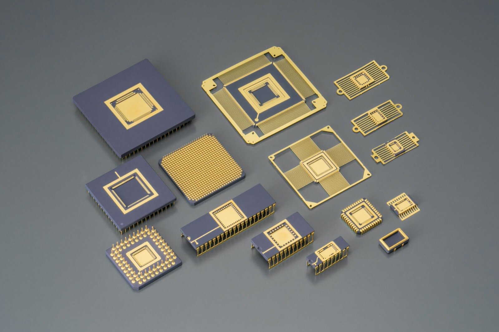
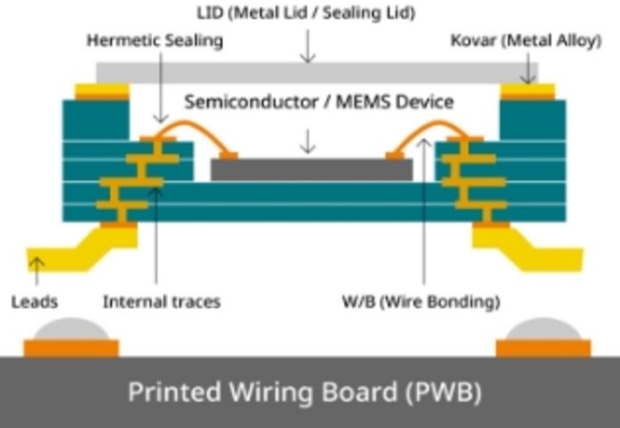
The role of ceramic packages
- It protects the IC chip from external environmental factors (water vapor, dust, light, electromagnetic waves, radiation, etc.) and temperature.
- To facilitate the assembly of IC chips.
- It transmits electrical signals from IC chips without losing any signal.
- It dissipates the heat generated from the IC chip.
Product Introduction Video
For inquiries regarding this product, please contact us here.
Related Products
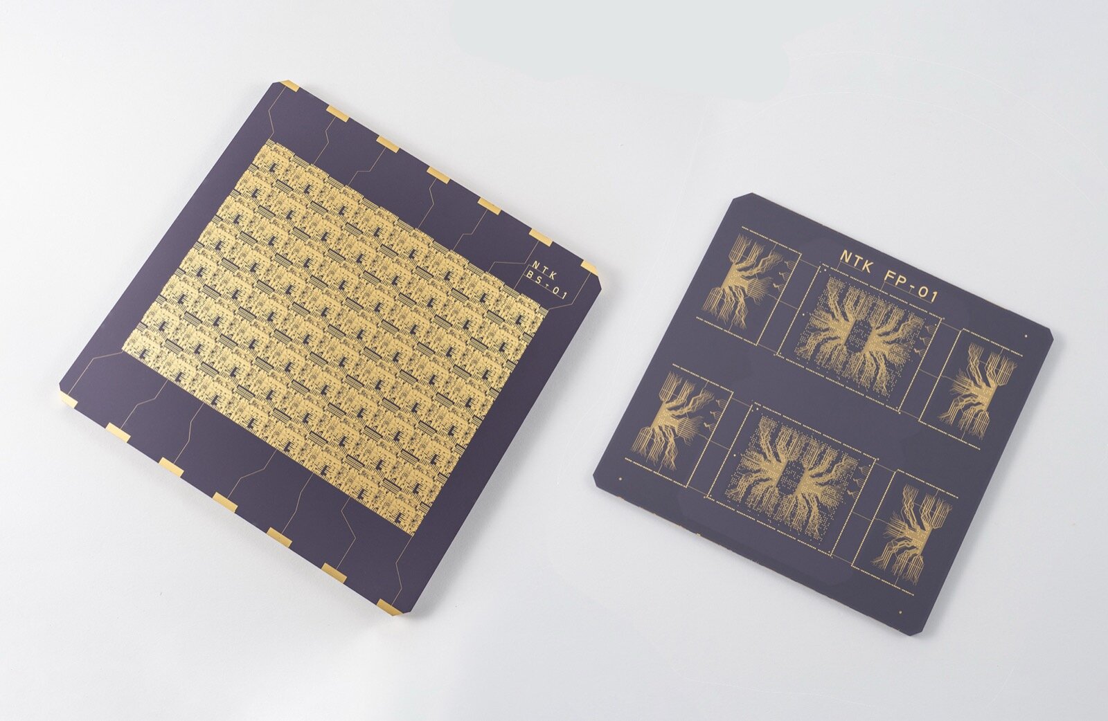 High-precision, high-density ceramic substrates used in probe cards that support semiconductor testing.
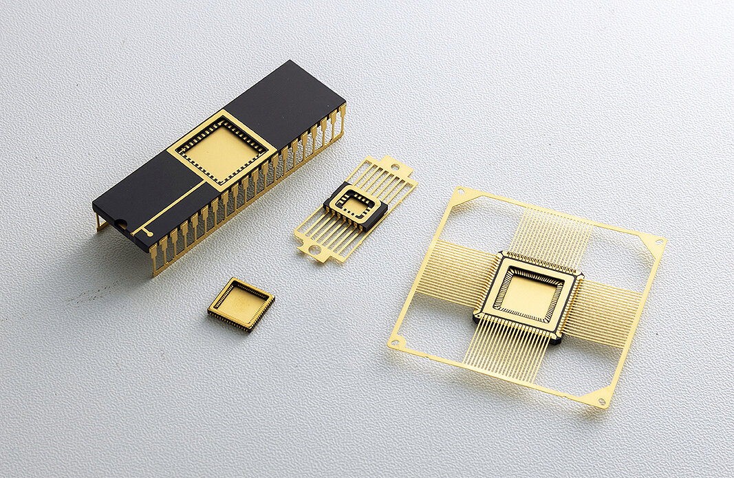 Ceramic packages that support the long-term stable operation, high-precision control, and excellent signal quality required for microcontrollers and analog ICs.
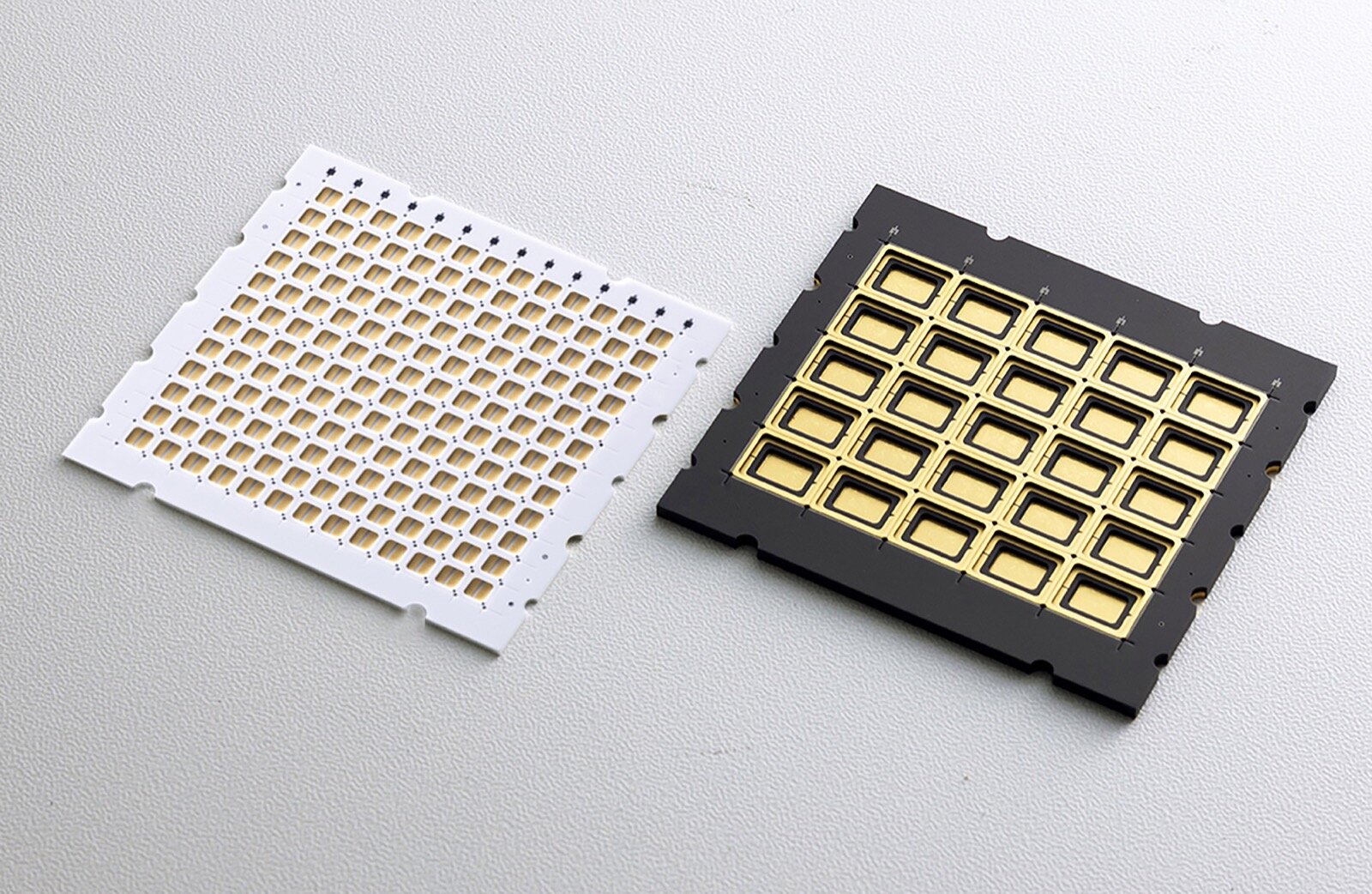 Ceramic packages with the heat dissipation and environmental resistance needed to maximize the irradiation performance of optical semiconductors.
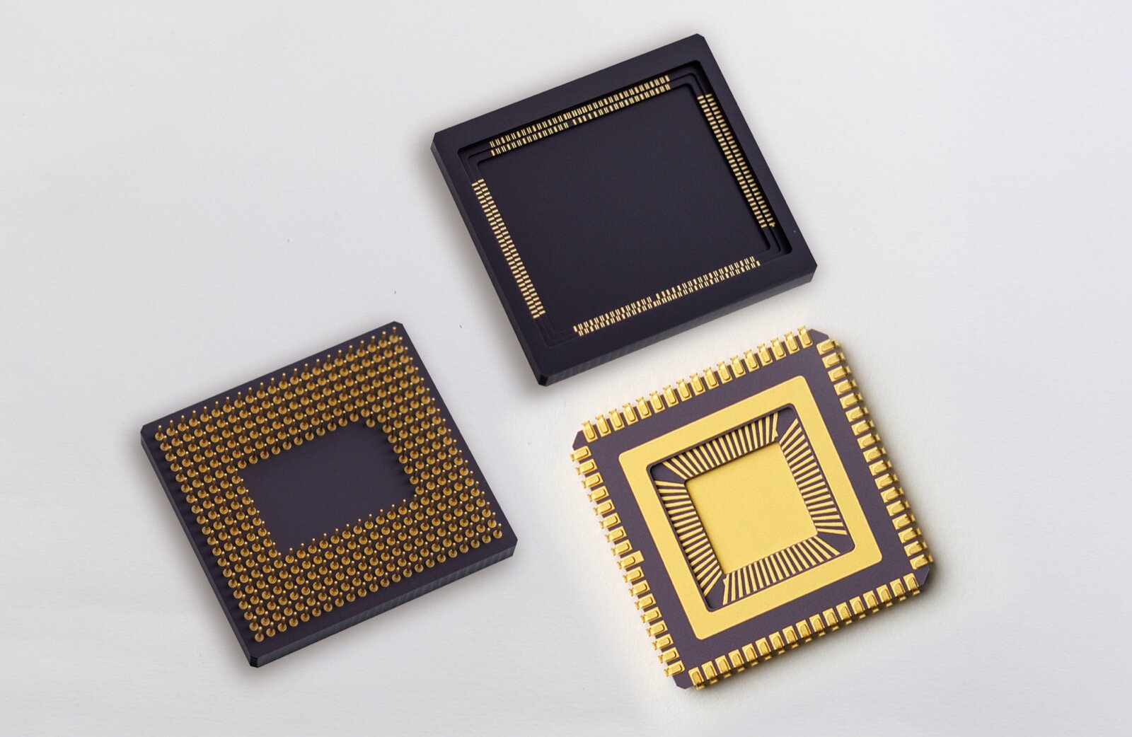 Ceramic packages with excellent flatness and high rigidity that support precise sensing in image sensors as they advance toward higher resolution, higher speed, and more sophisticated sensing.
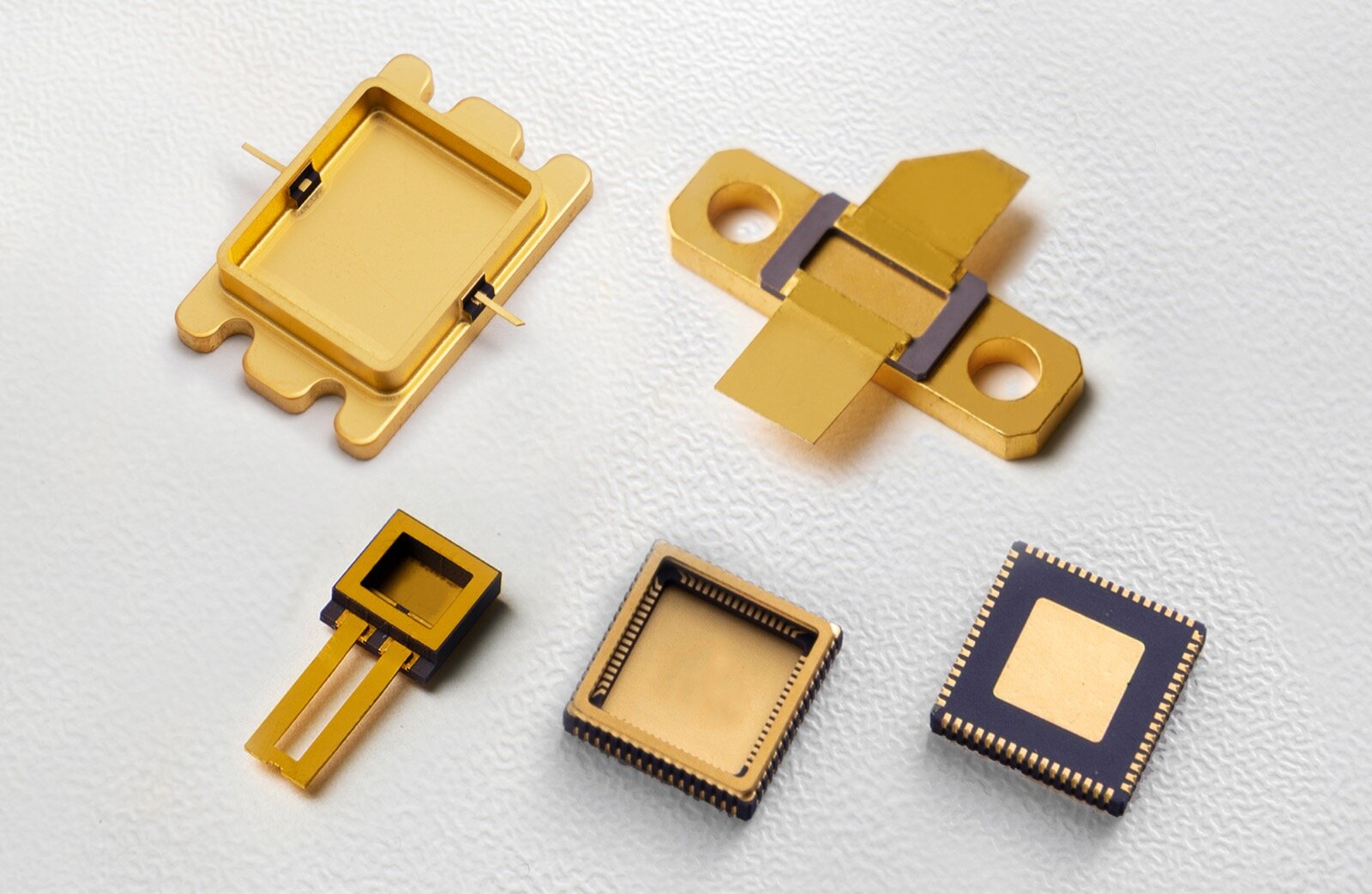 Ceramic packages that dissipate the intense heat generated by high-current and high-frequency operation, minimize signal loss with excellent electrical characteristics, and support stable system operation.
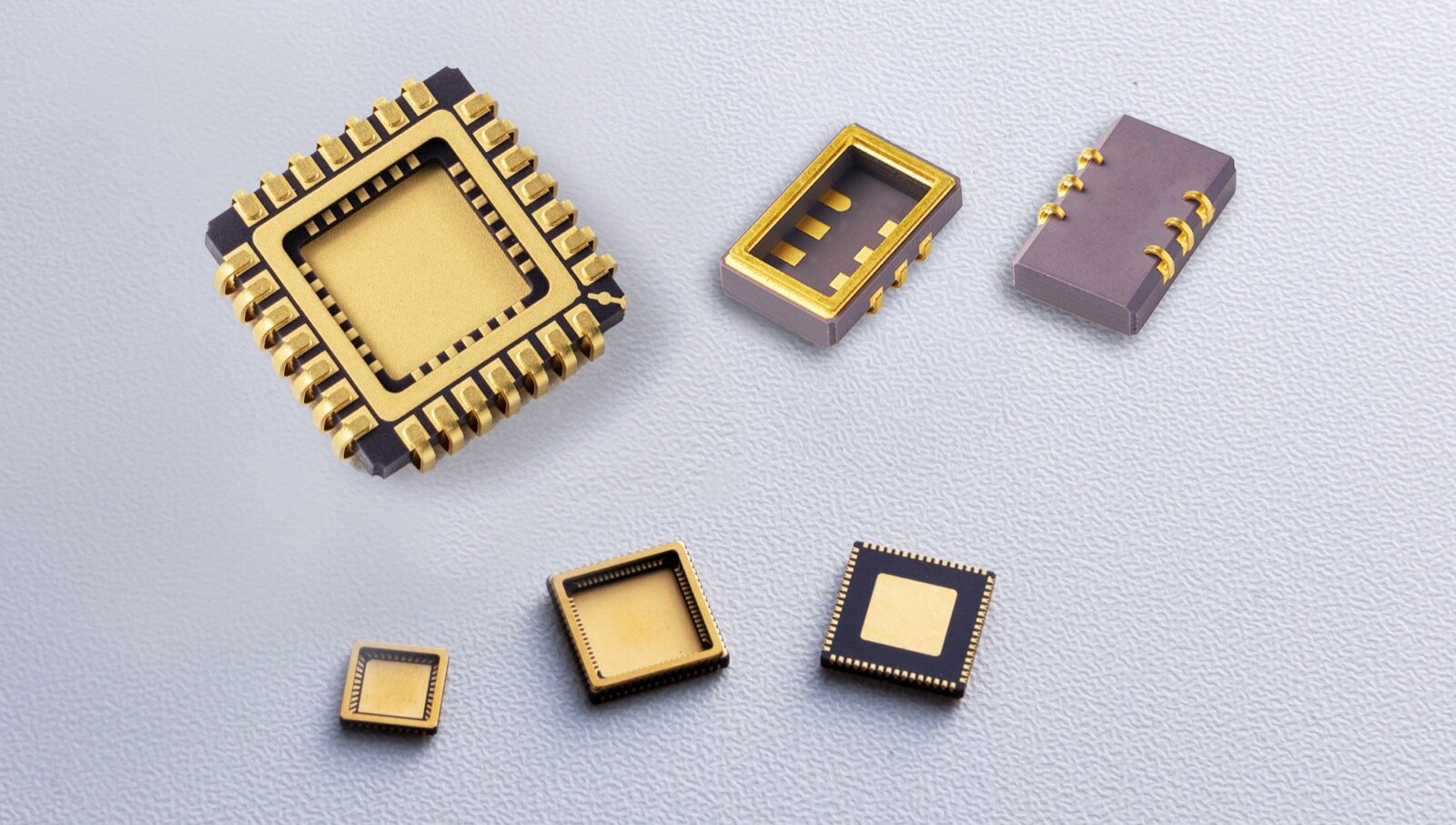 Ceramic packages with high hermeticity to protect fine structures and excellent environmental resistance, supporting the reliable operation of a wide range of sensors and devices.
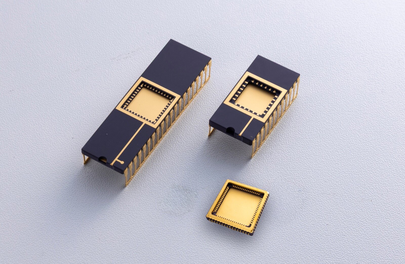 Ceramic packages that achieve stable connection with testers and excellent dimensional accuracy in demanding burn-in tests and high-speed signal characterization, reliably supporting the evaluation of advanced semiconductors.
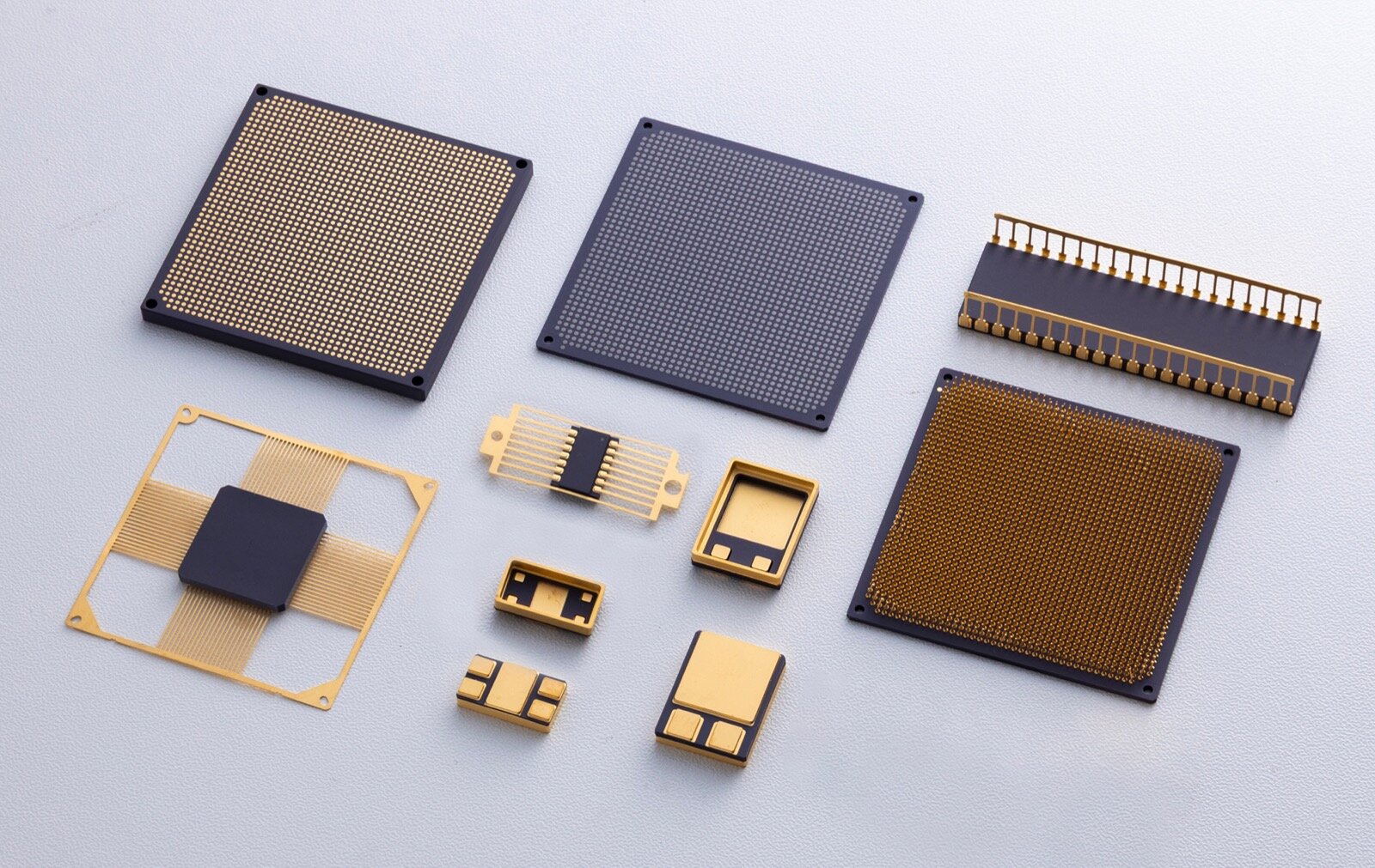 Multilayer Ceramic Substrates with excellent thermal stability and reliable chip bonding for high-density devices in communications, industrial, and medical applications, supporting stable operation even in harsh environments.